| CPC H10K 50/868 (2023.02) [G02B 5/305 (2013.01); G02B 5/3083 (2013.01); H01L 27/1225 (2013.01); H01L 29/78672 (2013.01); H01L 29/7869 (2013.01); H10K 50/844 (2023.02); H10K 59/123 (2023.02); H10K 59/40 (2023.02); H10K 59/8791 (2023.02); H10K 71/00 (2023.02); H10K 59/1201 (2023.02); H10K 59/8723 (2023.02); H10K 59/8731 (2023.02)] | 17 Claims |
|
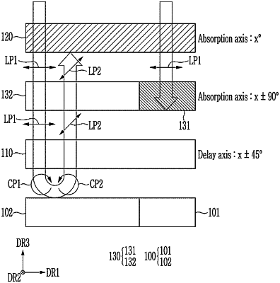
1. A light emitting display device comprising:
a display panel including a light emitting area and a non-light emitting area;
a phase delay layer disposed on an upper portion of the display panel; and
a polarizer and an additional polarizer disposed on an upper portion of the phase delay layer, wherein
the display panel includes:
a first transistor disposed on a substrate;
an organic film overlapping the first transistor and including an opening in a plan view;
a first electrode disposed on the organic film;
an emission layer disposed on the first electrode and disposed corresponding to the light emitting area; and
a second electrode disposed on the emission layer,
the first electrode, the emission layer, and the second electrode form a light emitting diode (LED),
the additional polarizer includes:
a polarization portion overlapping the opening of the organic film in a plan view; and
a non-polarization portion disposed in a region where the polarization portion is not disposed, and
the polarization portion is disposed in a portion of the non-light emitting area.
|