| CPC H10K 50/8426 (2023.02) [B23K 26/206 (2013.01); B32B 7/04 (2013.01); B32B 17/06 (2013.01); B32B 37/06 (2013.01); C03B 23/203 (2013.01); C03C 3/12 (2013.01); C03C 3/14 (2013.01); C03C 3/16 (2013.01); C03C 3/23 (2013.01); C03C 3/247 (2013.01); C03C 4/0071 (2013.01); C03C 8/24 (2013.01); C03C 23/0025 (2013.01); C03C 27/06 (2013.01); C03C 27/08 (2013.01); H10K 71/50 (2023.02); B32B 2250/03 (2013.01); B32B 2250/40 (2013.01); B32B 2255/20 (2013.01); B32B 2310/0825 (2013.01); B32B 2310/0831 (2013.01); B32B 2310/0843 (2013.01); B32B 2457/206 (2013.01); C03C 2204/00 (2013.01); C03C 2207/00 (2013.01); C03C 2218/32 (2013.01); H10K 2102/00 (2023.02)] | 20 Claims |
|
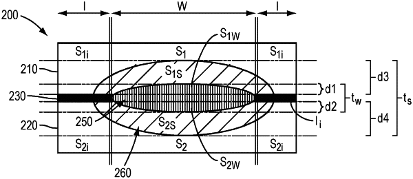
1. A sealed device comprising:
a first substrate including a first surface;
a second substrate including a second surface;
an inorganic film disposed between the first surface and the second surface, the inorganic film including;
a welded portion having a weld region comprising a bond formed between the first and second substrates and extending from a first depth in the first substrate to a second depth in the second substrate; and
a non-welded portion;
wherein the inorganic film comprises at least one inorganic film element and wherein one or both of the first and second substrates comprises at least one inorganic substrate element; and
wherein a first inorganic film element concentration of the first or second substrate in the weld region is higher than a second inorganic film element concentration of the first or second substrate outside the weld region; and
wherein the inorganic film, and optionally at least one of the first or second substrates is transmissive at wavelengths ranging from about 420 nm to about 750 nm.
|