| CPC H10K 19/202 (2023.02) [H10K 10/50 (2023.02); H10K 85/221 (2023.02)] | 20 Claims |
|
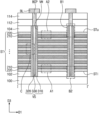
1. A variable resistance memory device, comprising:
a stack including insulating sheets and conductive sheets, which are alternatingly stacked on a substrate, the stack including a vertical hole vertically penetrating therethrough;
a bit line on the stack;
a conductive pattern electrically connected to the bit line and vertically extending in the vertical hole; and
a resistance varying layer between the conductive pattern and an inner side surface of the stack defining the vertical hole,
wherein the resistance varying layer comprises a first carbon nanotube electrically connected to the conductive sheets, and a second carbon nanotube electrically connected to the conductive pattern.
|