| CPC H10H 20/857 (2025.01) [H01L 25/0753 (2013.01); H10H 20/0364 (2025.01)] | 13 Claims |
|
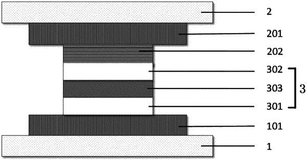
1. A μLED light-emitting and display device with single-ended electrical contact and single-ended carrier injection, comprising more than one pixel unit, and each pixel unit sequentially comprising a lower pixel electrode, μLED chips, an insulating layer, and an upper pixel electrode from bottom to top, wherein the μLED chips directly contact with the lower pixel electrode, external carriers are injected into the μLED chips through the lower pixel electrode, the insulating layer prevents the external carriers from being injected into the μLED chips through the upper pixel electrode, and the μLED chips are lit by an alternating electric field applied between the upper pixel electrode and the lower pixel electrode;
μLED chips comprise a P-type semiconductor layer, a light-emitting layer and a N-type semiconductor layer, and the P-type semiconductor layer, the light-emitting layer and the N-type semiconductor layer are stacked to form a semiconductor junction capable of emitting light under the action of an electric field;
wherein the semiconductor junction in the μLED chips comprises a single PN junction, a single heterojunction, a composite PN junction comprising a plurality of PN junctions, or a combined semiconductor junction comprising a PN junction and a heterojunction;
wherein the semiconductor junction is located on the surface or in the inside of the μLED chips.
|