| CPC H10F 77/147 (2025.01) [H10F 71/1215 (2025.01); H10F 30/225 (2025.01); H10F 77/122 (2025.01); H10F 77/241 (2025.01); H10F 77/306 (2025.01)] | 5 Claims |
|
1. An ultraviolet detector, comprising:
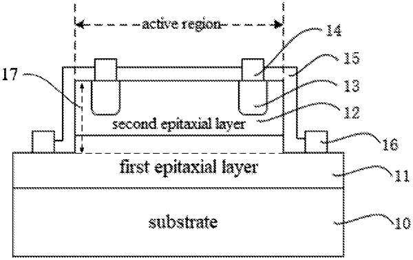
a substrate;
a first epitaxial layer located on the substrate, the first epitaxial layer being a heavily doped epitaxial layer with a doping concentration between 1×1018 cm−3˜1×1020 cm−3;
a second epitaxial layer located on the first epitaxial layer, the second epitaxial layer being a lightly doped epitaxial layer with a doping concentration between 1×1015 cm−3˜1×1017 cm−3, or the second epitaxial layer being a double-layer or multi-layer structure comprising at least one lightly doped epitaxial layer with a doping concentration between 1×1015 cm−3˜1×1017 cm−3 and at least one heavily doped epitaxial layer with a doping concentration between 5×1017 cm−3˜1×1020 cm−3;
an ohmic contact layer located on the second epitaxial layer or formed in the second epitaxial layer, the ohmic contact layer being a graphical heavily doped layer with a doping concentration between 1×1018 cm−3˜1×1020 cm−3, wherein when the ohmic contact layer is formed in the second epitaxial layer, an upper surface of the ohmic contact layer is not lower than an upper surface of the second epitaxial layer, and a lower surface of the ohmic contact layer is higher than a lower surface of the second epitaxial layer, and wherein a surface graphic of the ohmic contact layer includes a window shape or an array shape; and
a first metal electrode layer, a surface area of the first metal electrode layer touching the ohmic contact layer is not larger than a surface area of the ohmic contact layer, the surface area of the first metal electrode layer is a connected area; when the surface graphic of the ohmic contact layer is the window shape, the first metal electrode layer is entirely located on and in contact with the ohmic contact layer, and a surface graphic of the first metal electrode layer is the window shape; and when the surface graphic of the ohmic contact layer is the array shape, a portion of the first metal electrode layer is located on and in contact with the ohmic contact layer, a connection portion of the first metal electrode layer is located above the second epitaxial layer, and the surface graphic of the first metal electrode layer is the array shape; and
wherein the ultraviolet detector further comprises a passivation protection layer that covers an area on an outer surface of the second epitaxial layer without covering an outer surface of the first metal electrode layer;
wherein a surface area of the second epitaxial layer is smaller than a surface area of the first epitaxial layer, and the second epitaxial layer and a partial area on the first epitaxial layer together form an isolation mesa, and wherein the partial area represents a region within which the second epitaxial layer is located on the first epitaxial layer; and
the ultraviolet detector further comprises a second metal electrode layer, and the second metal electrode layer is formed on an area on the first epitaxial layer other than the isolation mesa.
|