| CPC H10D 62/121 (2025.01) [H10D 30/031 (2025.01); H10D 30/6713 (2025.01); H10D 30/6735 (2025.01); H10D 30/6757 (2025.01); H10D 64/018 (2025.01)] | 20 Claims |
|
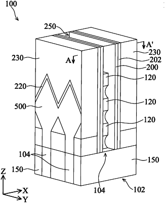
1. A semiconductor device, comprising:
a source/drain feature over a semiconductor substrate;
channel layers connected to the source/drain feature;
a gate structure between adjacent channel layers and wrapping the channel layers; and
an inner spacer between the source/drain feature and the gate structure and between adjacent channel layers,
wherein the source/drain feature has a first interface with a first channel layer of the channel layer, and the first interface has a convex profile protruding towards the first channel layer, and
wherein a height of the inner spacer is greater than a distance between the adjacent channel layers.
|