| CPC H10D 62/116 (2025.01) [H10D 62/151 (2025.01); H10D 62/235 (2025.01)] | 14 Claims |
|
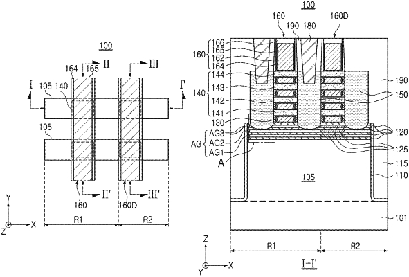
1. A semiconductor device comprising:
a substrate including an active region extending in a first direction;
a gate structure disposed on the substrate, intersecting the active region, and extending in a second direction;
a plurality of channel layers disposed on the active region and spaced apart in a third direction perpendicular to an upper surface of the substrate, wherein the plurality of channel layers are surrounded by the gate structure;
source/drain regions disposed on opposing sides of the gate structure and connected to the plurality of channel layers;
air gap regions disposed between the source/drain regions and the active region and spaced apart in the third direction; and
semiconductor layers below a lowermost channel layer of the plurality of channel layers and alternately disposed with the air gap regions in the third direction to define the air gap regions,
wherein lower ends of the source/drain regions are located at a level lower than an uppermost air gap region among the air gap regions.
|