| CPC H10D 30/668 (2025.01) [H10D 30/0297 (2025.01); H10D 62/8503 (2025.01); H10D 64/513 (2025.01)] | 13 Claims |
|
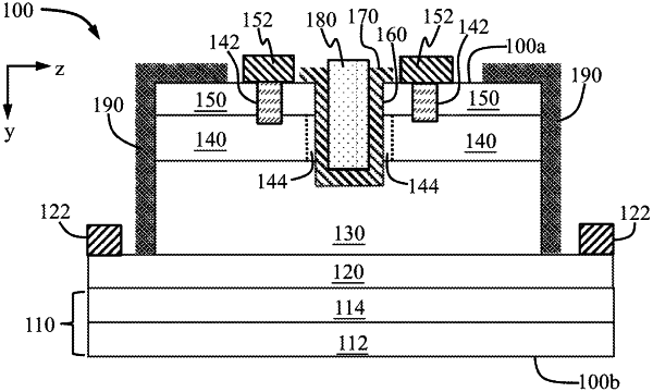
1. A GaN vertical trench MOSFET comprising a semiconductor transistor that has a first surface and a second surface, and a trench that extends from the first surface into the semiconductor transistor along a first direction perpendicular to the first and second surfaces, wherein the semiconductor transistor includes a body region having a channel region arranged along the first direction along at least a portion of a wall of the trench, and wherein a doping concentration of the channel region is non-uniform,
wherein the channel region includes a first portion and a second portion having an interface with the first portion, the interface being in parallel with the first and second surfaces, the doping concentration of the first portion being uniform across the first portion, the doping concentration of the second portion being uniform across the second portion, the doping concentration of the second portion being greater than the doping concentration of the first portion,
wherein the semiconductor transistor comprises a source region, and the source region is disposed on the body region and comprises the first surface,
wherein the second portion is sandwiched between the source region and the first portion,
wherein the first portion and the second portion are doped with a same type of dopants.
|