| CPC H10B 80/00 (2023.02) [H01L 23/49816 (2013.01); H01L 23/5383 (2013.01); H01L 24/16 (2013.01); H01L 25/0655 (2013.01); H03K 19/1776 (2013.01); H01L 2224/16227 (2013.01)] | 25 Claims |
|
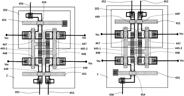
1. A multichip package comprising:
an interconnection scheme;
a first metal bump under and coupling to the interconnection scheme and at a bottom of the multichip package;
a semiconductor integrated-circuit (IC) chip over the interconnection scheme and coupling to the first metal bump through the interconnection scheme, wherein the semiconductor integrated-circuit (IC) chip is field-programmable; and
a non-volatile memory (NVM) integrated-circuit (IC) chip over the interconnection scheme, wherein the non-volatile memory (NVM) integrated-circuit (IC) chip comprises a first data terminal coupling to a first data terminal of the semiconductor integrated-circuit (IC) chip through the interconnection scheme and a read-enable terminal coupling to a first input/output (I/O) terminal of the semiconductor integrated-circuit (IC) chip through the interconnection scheme, wherein the semiconductor integrated-circuit (IC) chip is configured to control the non-volatile memory (NVM) integrated-circuit (IC) chip and load first configuration data from the non-volatile memory (NVM) integrated-circuit (IC) chip to the semiconductor integrated-circuit (IC) chip when the multichip package is powered on, wherein the semiconductor integrated-circuit (IC) chip is configured to pass a read-enable signal from the first input/output (I/O) terminal of the semiconductor integrated-circuit (IC) chip to the read-enable terminal of the non-volatile memory (NVM) integrated-circuit (IC) chip to activate the first data terminal of the non-volatile memory (NVM) integrated-circuit (IC) chip for passing the first configuration data from the first data terminal of the non-volatile memory (NVM) integrated-circuit (IC) chip to the first data terminal of the semiconductor integrated-circuit (IC) chip for configuring the semiconductor integrated-circuit (IC) chip in accordance with data associated with the first configuration data, wherein the read-enable terminal of the non-volatile memory (NVM) integrated-circuit (IC) chip and the first input/output (I/O) terminal of the semiconductor integrated-circuit (IC) chip are coupled to each other through a first path starting from the first input/output (I/O) terminal of the semiconductor integrated-circuit (IC) chip to the read-enable terminal of the non-volatile memory (NVM) integrated-circuit (IC) chip, wherein the first path is completely buried in one or more insulating dielectric materials of the multichip package and has no electrical contact at all surfaces of the multichip package.
|