| CPC H10B 63/84 (2023.02) [H10B 63/24 (2023.02); H10N 70/063 (2023.02); H10N 70/231 (2023.02)] | 10 Claims |
|
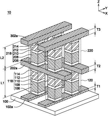
1. A memory device, comprising:
a substrate;
a first conductive stripe disposed on the substrate and extending along a first direction;
a second conductive stripe disposed on the first conductive stripe and extending along a second direction, wherein the first direction and the second direction are parallel to an upper surface of the substrate, and the second direction is intersected with the first direction, a thickness of the second conductive stripe is greater than a thickness of the first conductive stripe, and the second conductive stripe is an integral structure;
a first pillar element disposed at an intersection between the first conductive stripe and the second conductive stripe, and extending from a top surface of the first conductive stripe to a bottom surface of the second conductive stripe along a third direction, wherein the third direction is intersected with the first direction and the second direction, wherein the first pillar element comprises a switching layer and a memory layer corresponding to a first level; and
a spacer surrounding and directly contacting the first pillar element,
wherein the second conductive stripe has a same width in the first direction, and the spacer further surrounds the second conductive stripe to have a same width in the first direction.
|