| CPC H10B 43/35 (2023.02) [H01L 23/5226 (2013.01); H10B 43/10 (2023.02); H10B 43/20 (2023.02); H01L 2924/1438 (2013.01); H01L 2924/145 (2013.01)] | 20 Claims |
|
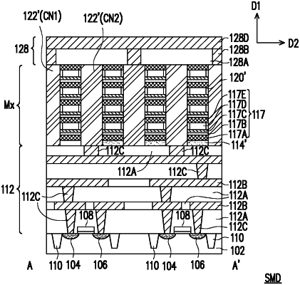
1. A structure, comprising:
an interconnection layer;
a plurality of memory stacks disposed on the interconnection layer, wherein each of the plurality of memory stacks comprises a channel layer, a charge trapping layer disposed on the channel layer, and a gate layer disposed on the charge trapping layer, and the plurality of memory stacks are stacked up to form a column structure, wherein the channel layer in each of the plurality of memory stacks are physically separated from one another;
connecting lines disposed on two sides of the column structure, wherein a first portion of the connecting lines is electrically connected to the interconnection layer; and
a second interconnection layer disposed on the plurality of memory stacks and on the connection lines, wherein the second interconnection layer is electrically connected to a second portion of the connecting lines.
|