| CPC H10B 43/27 (2023.02) [H10B 43/10 (2023.02); H10B 43/30 (2023.02)] | 20 Claims |
|
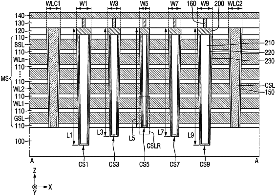
1. A nonvolatile memory device comprising:
a substrate;
a mold structure including a plurality of word lines stacked on the substrate;
a first word line cut region cutting the mold structure;
a first channel structure apart from the first word line cut region by a first distance, and in the mold structure and the substrate; and
a second channel structure apart from the first word line cut region by a second distance, and in the mold structure and the substrate,
wherein the second distance is greater than the first distance,
a first width of the first channel structure is different from a second width of the second channel structure, and
a first length of the first channel structure is different from a second length of the second channel structure.
|