| CPC H10B 10/12 (2023.02) [G11C 11/412 (2013.01); H01L 23/5384 (2013.01); H01L 27/0886 (2013.01); H01L 29/785 (2013.01); H01L 2029/7858 (2013.01)] | 20 Claims |

|
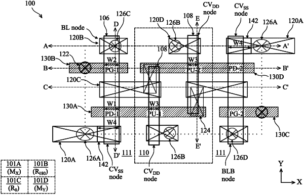
1. An integrated circuit (IC) structure, comprising:
a first static random-access memory (SRAM) cell, including:
a first pull-down (PD) device and a second PD device disposed over a first fin and a second fin, respectively,
wherein a portion of the first fin and a portion of the second fin corresponding to a channel region of the first and the second PD devices, respectively, each include a first stack of semiconductor layers defined by a channel width W1, and
wherein a portion of the first fin and a portion of the second fin providing a source terminal of the first and the second PD devices, respectively, are each defined by a width W1′ that is enlarged with respect to the channel width W1 by a first difference,
wherein the first PD device and the second PD device each include an epitaxial source/drain feature over the source terminal; and
a second SRAM cell disposed adjacent to the first SRAM cell, wherein a layout of the second SRAM cell is a mirror image of a layout of the first SRAM cell about a cell boundary disposed therebetween, and wherein the enlargement of the width W1′ with respect to the channel width W1 extends laterally toward the second SRAM cell.
|