US 12,267,963 B2
Circuit board with anti-corrosion properties and electronic device having the same
Li-Ping Wang, Foshan (CN); Yung-Ping Lin, New Taipei (TW); Yong-Kang Zhang, Shenzhen (CN); Qiu-Ri Zhang, New Taipei (TW); and You-Zhi Lu, Foshan (CN)
Assigned to CHAMP TECH OPTICAL (FOSHAN) CORPORATION, Foshan (CN)
Filed by CHAMP TECH OPTICAL (FOSHAN) CORPORATION, Foshan (CN)
Filed on Jan. 31, 2024, as Appl. No. 18/428,187.
Application 18/428,187 is a division of application No. 17/740,975, filed on May 10, 2022, granted, now 11,943,875.
Claims priority of application No. 202110711063.8 (CN), filed on Jun. 25, 2021.
Prior Publication US 2024/0172370 A1, May 23, 2024
Int. Cl. H05K 1/02 (2006.01); H01L 23/544 (2006.01); H01L 33/10 (2010.01); H01L 33/38 (2010.01); H01L 33/54 (2010.01); H01L 33/56 (2010.01); H01L 33/58 (2010.01); H01L 33/60 (2010.01); H01L 33/62 (2010.01); H05K 3/00 (2006.01); H05K 3/10 (2006.01); H05K 3/12 (2006.01); H05K 3/22 (2006.01); H05K 3/28 (2006.01)
CPC H05K 3/282 (2013.01) [H05K 3/0091 (2013.01); H05K 3/103 (2013.01)] 3 Claims
OG exemplary drawing
 
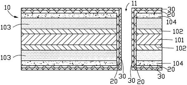
1. A circuit board comprising:
a circuit substrate comprising a base layer and an outer wiring layer formed on the base layer, and a via hole connected to the outer wiring layer;
a first protective layer made of white oil and formed on the outer wiring layer and an inner sidewall of the via hole;
a mark made of white oil and formed on the outer wiring layer by a silk-screen printing process, the silk-screen printing process further configured to form the first protective layer when printing the mark; and
a second protective layer made of a three proofing paint, the second protective layer formed on the first protective layer which is on the outer wiring layer, the second protective layer further formed on the first protective layer which is on the inner sidewall of the via hole.