| CPC H03F 1/42 (2013.01) [H03F 1/0205 (2013.01); H03F 1/565 (2013.01); H03F 2200/255 (2013.01); H03F 2200/451 (2013.01)] | 3 Claims |
|
1. A common-emitter amplifier with unilateral pre-embedding inductors, the common-emitter amplifier comprising:
an input matching circuit, a first-stage amplification circuit, a first-stage interstage matching circuit, a second-stage amplification circuit, a second-stage interstage matching circuit, a third-stage amplification circuit, a third-stage interstage matching circuit, and an output matching circuit;
wherein the common-emitter amplifier is configured to: make an input signal sequentially enter bases of common-emitter transistors of the first-stage, second-stage, and third-stage amplification circuits, make the input signal be amplified stage by stage by the common-emitter transistors, and finally make an amplified input signal obtained by amplifying of each of the common-emitter transistors output through a collector of each of the common-emitter transistors, as an output signal of each of the common-emitter transistors; and the common-emitter amplifier is further configured to introduce interstage staggered tuning to expand bandwidth to address a narrowband problem caused by resonance of inductance and capacitance;
wherein a miller capacitor (Cμ) between the base and the collector of each of the common-emitter transistors causes direct coupling between originally isolated input and output signals of each of the common-emitter transistors; and an amplitude of the output signal of the collector of each of the common-emitter transistors is closely related to a value of the miller capacitor (Cμ);
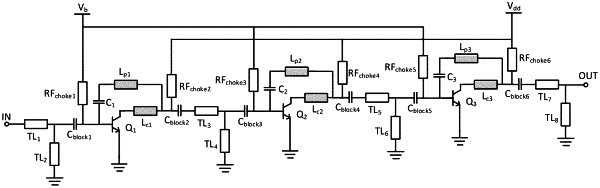
wherein a parallel embedding inductor (Lp) is introduced between the base and the collector of each of the common-emitter transistors, and is configured to resonate with the miller capacitor (Cμ) between the base and the collector of each of the common-emitter transistors thereby to eliminate an influence of the miller capacitor, improve the amplitude of the output signal of the collector of each of the common-emitter transistors, and increase a gain Gma of each of the common-emitter transistors to a maximum achievable gain Gmax at an operating frequency;
wherein the common-emitter amplifier further comprises the unilateral pre-embedding inductors, and each of the unilateral pre-embedding inductors is configured to reduce a required value of the parallel embedding inductor (Lp) between the base and collector of a corresponding one of the common-emitter transistors, thereby to reduce difficulty of implementing the parallel embedding inductor (Lp) between the base and the collector of the corresponding one of the common-emitter transistors;
wherein an admittance matrix of a first common-emitter transistor (Q1) of the common-emitter transistors is expressed as [Y11 Y12; Y21 Y22], an impedance of a first unilateral pre-embedding inductor (Lc) of the unilateral pre-embedding inductors is expressed as jXc, an admittance value of a parallel embedding network comprising the parallel embedding inductor (Lp) and a first capacitor (C1) is expressed as jBp, and an admittance matrix (Ytot) of a total network comprising the first common-emitter transistor (Q1), the first unilateral pre-embedding inductor (Lc), the parallel embedding inductor (Lp) and the first capacitor (C1) is as follows:
 wherein a transfer factor A of the total network is as follows:
 and a gain G of the total network is as follows:
 where K represents a stability coefficient;
wherein gains G of different networks are obtained by combining different unilateral pre-embedding inductors (Lc) and parallel embedding inductors (Lp), and an influence diagram of the gains of the total network of the different networks is plotted, when the gains all take peak values, an inductance value of the parallel embedding inductor (Lp) decreases with an increase of the unilateral pre-embedding inductor (Lc), which indicates that an introduction of the unilateral pre-embedding inductor (Lc) reduces the parallel embedding inductor (Lp).
|