| CPC H01P 3/16 (2013.01) [H01L 23/5384 (2013.01); H01L 23/66 (2013.01); H01L 25/0657 (2013.01); H01P 1/2088 (2013.01); H01P 5/107 (2013.01); H01L 2223/6627 (2013.01)] | 22 Claims |
|
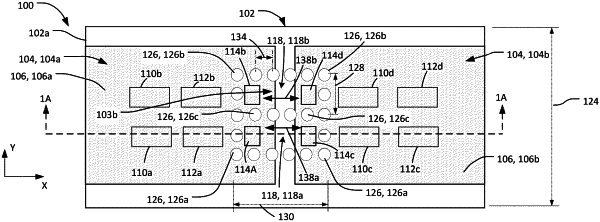
1. A semiconductor package comprising:
a first semiconductor die;
a second semiconductor die; and
a substrate positioned between the first semiconductor die and the second semiconductor die, the substrate including:
a waveguide interconnect to provide a communication channel to carry an electromagnetic signal, the waveguide interconnect defined by a plurality of through substrate vias (TSVs), the TSVs in a pattern around at least a portion of the substrate to define a boundary of the communication channel.
|