| CPC H01L 33/62 (2013.01) [H01L 27/156 (2013.01); H01L 33/005 (2013.01); H01L 33/38 (2013.01); H01L 2933/0066 (2013.01)] | 20 Claims |
|
1. A display device, comprising:
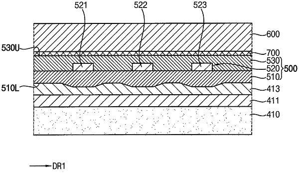
a display panel including an insulation layer and a pad disposed on the insulation layer; and
a driving unit including a bump electrically connected to the pad, wherein
the pad includes:
a first layer disposed directly on an upper surface of the insulation layer, the first layer including a conductive material;
a second layer disposed on the first layer, the second layer including a plurality of patterns arranged in a first direction and spaced apart from each other; and
a third layer disposed on the second layer, the third layer including a conductive material,
the first layer includes surface portions protruding toward the insulation layer and respectively corresponding to the plurality of patterns, and
the surface portions of the first layer are positioned above a lower surface of the insulation layer.
|