| CPC H01L 33/62 (2013.01) [H01L 25/0753 (2013.01)] | 20 Claims |
|
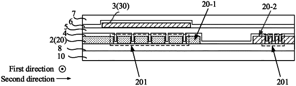
1. A display substrate, comprising:
a base substrate;
a first conductive layer, disposed on a side of the base substrate, wherein the first conductive layer comprises: a plurality of first conductive parts extending in a first direction and having different sizes in a second direction;
a second conductive layer, disposed on a side of the first conductive layer facing away from the base substrate; and
an insulation layer, disposed between the first conductive layer and the second conductive layer; wherein
at least two first conductive parts each comprise a first hollowed-out portion, the first hollowed-out portion comprises a plurality of groove structures distributed in the second direction and extending in the first direction, and the first direction and the second direction produce angles.
|