| CPC H01L 33/62 (2013.01) [H01L 27/156 (2013.01)] | 22 Claims |
|
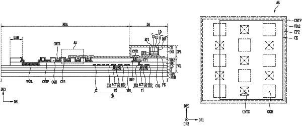
1. A display device comprising:
a substrate including a display area and a non-display area;
a pixel circuit portion disposed on the substrate and including both a bridge pattern and a transistor that drives a pixel overlapping the display area, the transistor including a gate electrode and at least one other electrode; and
a display element portion disposed on the pixel circuit portion and including a pixel electrode of the pixel, the pixel electrode being electrically connected to the at least one other electrode of the transistor through at least the bridge pattern, wherein
the pixel circuit portion includes a first capping layer disposed between and electrically connecting the bridge pattern and the pixel electrode,
the pixel electrode includes multiple metal layers,
the bridge pattern includes multiple metal layers,
at least one of the multiple metal layers of the pixel electrode includes a same material as at least one of the multiple metal layers of the bridge pattern, and
the first capping layer includes a material different from materials of the multiple metal layers of the pixel electrode and a layer among the multiple metal layers of the bridge pattern that is closest to the pixel electrode.
|