| CPC H01L 33/62 (2013.01) [H01L 33/005 (2013.01); H01L 33/38 (2013.01); H01L 2933/0066 (2013.01)] | 9 Claims |
|
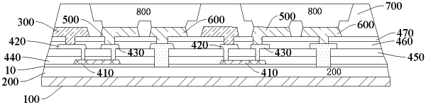
1. A light-emitting substrate, comprising:
a base substrate;
a first signal line located at one side of the base substrate;
an insulation layer located at one side of the first signal line away from the base substrate;
an electrode layer located at one side of the insulation layer away from the base substrate and comprising a first electrode terminal, a second electrode terminal and a second signal line, the first electrode terminal being electrically connected to the first signal line via a first through hole penetrating the insulation layer; and
at least one light-emitting element bound and connected to the first electrode terminal and the second electrode terminal;
wherein the first signal line and the second signal line are arranged at different layers;
wherein the light-emitting substrate further comprises a thin film transistor layer located between the first signal line and the electrode layer, wherein the thin film transistor layer comprises:
an active layer located at the one side of the first signal line away from the base substrate;
a first insulation layer covering the active layer and located at one side of the active layer away from the base substrate;
a source/drain metal layer located at one side of the first insulation layer away from the base substrate, wherein source and drain electrodes in the source/drain metal layer are connected to the active layer via second through holes penetrating the first insulation layer; and
a second insulation layer located at one side of the source/drain metal layer away from the first insulation layer, wherein the second signal line is connected to one of the source and drain electrodes via a third through hole penetrating the second insulation layer, and the second electrode terminal is connected to the other of the source and drain electrodes via a fourth through hole penetrating the second insulation layer;
wherein the insulation layer comprises the first insulation layer and the second insulation layer;
wherein the first through hole comprises:
a first sub through hole extending from the electrode layer to the source/drain metal layer; and
a second sub through hole extending from the source/drain metal layer to the first signal line;
wherein an orthographic projection of the first sub through hole onto the base substrate is within an orthographic projection of the second sub through hole onto the base substrate, the orthographic projection of the first sub through hole onto the base substrate is smaller than the orthographic projection of the second sub through hole onto the base substrate, and a diameter of the first sub through hole is smaller than a diameter of the second sub through hole;
wherein an alloy buffer layer is further provided between the base substrate and the first signal line;
wherein both a material of which the first signal line is made and a material of which the second signal line is made comprise Cu;
wherein a thickness of the first signal line and a thickness of the second signal line each ranges from 1.5 μm to 2.5 μm;
wherein a line width of the first signal line and a line width of the second signal line are each not less than 100 μm;
wherein the light-emitting substrate further comprises a buffer layer between the thin film transistor layer and the first signal line;
wherein the buffer layer has a thickness greater than 0.3 μm.
|
|
6. A method for forming a light-emitting substrate, comprising:
forming a first signal line on one side of a base substrate;
forming an insulation layer on one side of the first signal line away from the base substrate;
forming an electrode layer on one side of the insulation layer away from the base substrate,
wherein the electrode layer comprises a first electrode terminal, a second electrode terminal and a second signal line;
enabling the first electrode terminal of the electrode layer to be electrically connected to the first signal line via a first through hole penetrating the insulation layer; and
binding at least one light-emitting element to the first electrode terminal and the second electrode terminal;
wherein the light-emitting substrate further comprises a thin film transistor layer located between the first signal line and the electrode layer, the thin film transistor layer comprises an active layer, a first insulation layer, a source/drain metal layer and a second insulation layer, and the enabling the first electrode terminal of the electrode layer to be electrically connected to the first signal line via the first through hole penetrating the insulation layer, comprises:
forming the active layer and the first insulation layer successively on the one side of the first signal line away from the base substrate; wherein a second sub through hole is formed in the first insulation layer;
forming the source/drain metal layer on one side of the first insulation layer away from the base substrate, and filling a material of which the source/drain metal layer is made in the second sub through hole;
forming the second insulation layer on one side of the source/drain metal layer away from the base substrate, wherein a first sub through hole is formed in the second insulation layer; and
forming the electrode layer and filling a material of which the electrode layer is made in the first sub through hole; wherein the first electrode terminal is electrically connected to the first signal line through the material of which the source/drain metal layer is made in the second sub through hole and the material of which the electrode layer is made in the first sub through hole;
wherein an orthographic projection of the first sub through hole onto the base substrate is within an orthographic projection of the second sub through hole onto the base substrate, the orthographic projection of the first sub through hole onto the base substrate is smaller than the orthographic projection of the second sub through hole onto the base substrate, and a diameter of the first sub through hole is smaller than a diameter of the second sub through hole;
wherein an alloy buffer layer is further provided between the base substrate and the first signal line;
wherein both a material of which the first signal line is made and a material of which the second signal line is made comprise Cu;
wherein a thickness of the first signal line and a thickness of the second signal line each ranges from 1.5 μm to 2.5 μm;
wherein a line width of the first signal line and a line width of the second signal line are each not less than 100 μm;
wherein the light-emitting substrate further comprises a buffer layer between the thin film transistor layer and the first signal line;
wherein the buffer layer has a thickness greater than 0.3 μm.
|