| CPC H01L 33/60 (2013.01) [H01L 33/507 (2013.01); H01L 27/156 (2013.01)] | 20 Claims |
|
1. A semiconductor light-emitting device comprising:
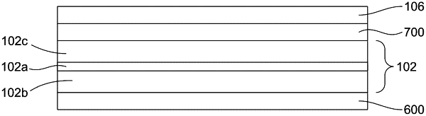
a semiconductor diode structure including first and second doped semiconductor layers and an active layer between a back surface of the first semiconductor layer and a front surface of the second semiconductor layer, the active layer being arranged for emitting diode output light, resulting from electrical current flow through the diode structure, at a nominal emission vacuum wavelength λ0 to propagate within the diode structure;
a reflector positioned against a back surface of the second semiconductor layer that internally reflects diode output light incident thereon from within the diode structure;
a wavelength-converting layer positioned with a back surface thereof facing and spaced-apart from a front surface of the first semiconductor layer, the wavelength-converting layer absorbing diode output light at the vacuum wavelength λ0 and in response emitting down-converted light at a vacuum wavelength λ1 that is greater than λ0, at least a portion of the down-converted light exiting the wavelength-converting layer through a front surface thereof; and
an intermediate spacer positioned between the front surface of the first semiconductor layer and the back surface of the wavelength-converting layer and comprising one or more dielectric layers, each dielectric layer of the intermediate spacer being at least partly transparent at the vacuum wavelength λ0, the intermediate spacer having an effective refractive index nS less than an effective refractive index nC of the wavelength-converting layer so that the wavelength-converting layer acts as an optical waveguide supporting one or more laterally propagating optical modes at the vacuum wavelengths λ0 and λ1.
|