| CPC H01L 33/44 (2013.01) [H01L 25/0753 (2013.01); H01L 25/167 (2013.01); H01L 33/007 (2013.01); H01L 33/0075 (2013.01); H01L 33/0093 (2020.05); H01L 33/62 (2013.01); H01L 2933/0025 (2013.01)] | 3 Claims |
|
1. A method of manufacturing a light emitting element, the method comprising:
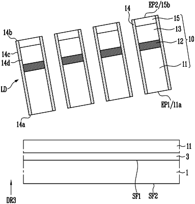
forming a light emitting stack structure by sequentially stacking a first semiconductor layer, an active layer, a second semiconductor layer, and an additional electrode on a substrate;
forming at least one light emitting stack pattern by etching the light emitting stack structure in a vertical direction, and exposing one region of the first semiconductor layer to the outside;
coating an insulating material layer made of a zinc acetate solution on the light emitting stack pattern by using a wet chemical process and drying the coated insulating material layer;
forming an insulating film surrounding an outer surface of the light emitting stack pattern by etching the dried insulating material layer in the vertical direction; and
forming the light emitting element by separating the light emitting stack pattern surrounded by the insulating film from the substrate.
|