| CPC H01L 33/38 (2013.01) [H01L 25/0753 (2013.01); H01L 27/156 (2013.01); H01L 33/62 (2013.01)] | 16 Claims |
|
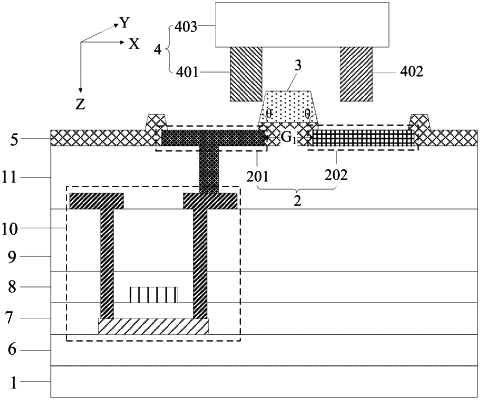
1. A driving backplane, comprising:
a base substrate;
a plurality of connection electrode groups disposed on the base substrate; and
a plurality of correction structures disposed on the base substrate;
wherein each of the connection electrode groups comprises:
a first connection electrode; and
a second connection electrode;
wherein the first connection electrode and the second connection electrode are arranged on a same layer;
a first gap is formed between the first connection electrode and the second connection electrode;
an edge of the first connection electrode in contact with the first gap and an edge of the second connection electrode in contact with the first gap form a first group of opposite edges;
an edge of the first connection electrode away from the first gap and an edge of the second electrode away from the first gap form a second group of opposite edges;
wherein an orthographic projection, on the base substrate, of each of the correction structures overlaps with an orthographic projection, on the base substrate, of one group of opposite edges, wherein the one group of opposite edges is the first group of opposite edges or the second group of opposite edges;
slope angles of the each of the correction structures at the one group of opposite edges are acute angles; and
the each of the correction structures is configured to limit a first electrode and a second electrode of a micro-LED to a surface of the first connection electrode and a surface of the second connection electrode comprised in the each of the connection electrode groups respectively;
wherein the plurality of correction structures are on a side, facing away from the base substrate, of a layer where the plurality of connection electrode groups are arranged; and
the orthographic projection, on the base substrate, of the each of the correction structures is coincide with an orthographic projection, on the base substrate, of the first group of opposite edges and an orthographic projection, on the base substrate, of the first gap;
wherein the driving backplane further comprises:
an insulation layer disposed between a layer where the plurality of correction structures are arranged and the layer where the plurality of connection electrode groups are arranged; wherein
the insulation layer is provided with a plurality of openings, and an orthographic projection, on the base substrate, of each of the openings is in an orthographic projection of the first connection electrode and an orthographic projection of the second connection electrode.
|