| CPC H01L 29/785 (2013.01) [H01L 21/0214 (2013.01); H01L 21/02211 (2013.01); H01L 21/02263 (2013.01); H01L 21/76224 (2013.01); H01L 21/76232 (2013.01); H01L 21/823481 (2013.01); H01L 27/0924 (2013.01); H01L 29/517 (2013.01); H01L 29/66545 (2013.01); H01L 29/66795 (2013.01); H01L 29/66818 (2013.01); H01L 21/76227 (2013.01)] | 20 Claims |
|
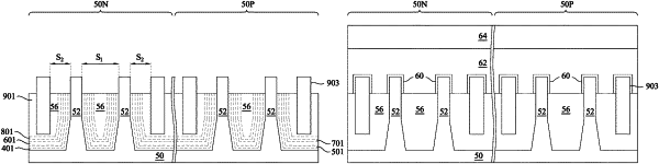
1. A semiconductor device comprising:
a first liner extending between a first semiconductor fin and a second semiconductor fin over a semiconductor substrate;
a second liner in physical contact with the first liner;
a third liner in physical contact with the second liner, the third liner comprising nitrogen at a percentage of less than about 10%;
a fourth liner in physical contact with the third liner;
a capping layer in physical contact with the fourth liner, the capping layer comprising carbon at a percentage of less than about 10%;
a dielectric cap in physical contact with the capping layer, wherein the first semiconductor fin extends further away from the semiconductor substrate than the dielectric cap; and
a dielectric fin embedded within the dielectric cap and extending further away from the semiconductor substrate than the dielectric cap.
|