| CPC H01L 29/7788 (2013.01) [H01L 29/0692 (2013.01); H01L 29/1037 (2013.01); H01L 29/205 (2013.01); H01L 29/66462 (2013.01); H01L 29/7783 (2013.01); H01L 29/2003 (2013.01)] | 9 Claims |

|
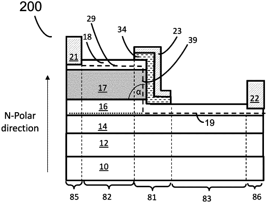
1. A III-N device, comprising:
a III-N material structure comprising a III-N channel layer over a III-N barrier layer, a p-type III-N layer over and directly contacting the III-N channel layer, and a 2DEG channel formed adjacent an interface between the III-N channel layer and the III-N barrier layer;
an n-type III-N layer over and directly contacting the p-type III-N layer,
a source electrode, a gate electrode, and a drain electrode each on a same side of the III-N material structure;
a gate insulator layer separating the gate electrode from the p-type III-N layer and the III-N channel layer; wherein
the source electrode directly contacts the n-type III-N layer and is electrically connected to the p-type III-N layer;
the drain electrode is electrically connected to the 2DEG channel;
a portion of the III-N channel layer separates the gate insulator layer from the III-N barrier layer;
the p-type III-N layer is over the III-N channel layer in a source side access region of the device and does not extend past the gate electrode; and
the 2DEG channel extends continuously through the III-N channel layer from below the source electrode to the drain electrode and the source electrode is electrically isolated from a portion of the 2DEG channel below the source electrode when the gate electrode is biased relative to the source electrode at a voltage that is below a threshold voltage of the device.
|