| CPC H01L 29/7786 (2013.01) [H01L 29/0642 (2013.01); H01L 29/2003 (2013.01); H01L 29/66462 (2013.01)] | 11 Claims |
|
1. A semiconductor device, comprising:
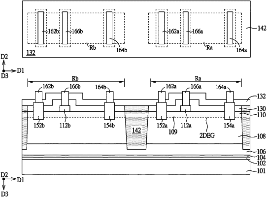
a substrate;
a buffer layer disposed on the substrate;
a channel layer disposed on the buffer layer;
a barrier layer disposed on the buffer layer;
a first semiconductor gate layer on the barrier layer;
a passivation layer disposed on the barrier layer and covering a top surface and sidewalls of the first semiconductor gate layer; and
a device isolation region enclosing a first device region of the semiconductor device and extending through the passivation layer and the barrier layer and into at least a portion of the channel layer, wherein a damage concentration of the device isolation region varies along a depth direction, and a depth range of a highest damage concentration covers a depth range of a two-dimensional electron gas layer at a junction between the barrier layer and the channel layer.
|