US 12,266,715 B2
Semiconductor devices and methods of manufacturing thereof
Shih-Yao Lin, New Taipei (TW); Chen-Ping Chen, Toucheng Township (TW); Kuei-Yu Kao, Hsinchu (TW); Hsiao Wen Lee, Hsinchu (TW); and Chih-Han Lin, Hsinchu (TW)
Assigned to Taiwan Semiconductor Manufacturing Company, Ltd., Hsinchu (TW)
Filed by Taiwan Semiconductor Manufacturing Company, Ltd., Hsinchu (TW)
Filed on Aug. 10, 2023, as Appl. No. 18/232,544.
Application 18/232,544 is a division of application No. 17/873,978, filed on Jul. 26, 2022, granted, now 11,923,440.
Application 17/873,978 is a division of application No. 17/081,877, filed on Oct. 27, 2020, granted, now 11,522,073.
Prior Publication US 2023/0387272 A1, Nov. 30, 2023
Int. Cl. H01L 29/94 (2006.01); H01L 21/8234 (2006.01); H01L 27/088 (2006.01); H01L 29/06 (2006.01); H01L 29/66 (2006.01); H01L 29/76 (2006.01); H01L 29/78 (2006.01)
CPC H01L 29/6681 (2013.01) [H01L 21/823431 (2013.01); H01L 21/823481 (2013.01); H01L 27/0886 (2013.01); H01L 29/0649 (2013.01); H01L 29/66545 (2013.01); H01L 29/785 (2013.01)] 20 Claims
OG exemplary drawing
 
1. A semiconductor device, comprising:
a substrate;
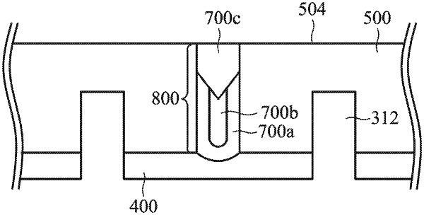
a dielectric isolation structure disposed on the substrate and having a horizontal upper surface;
semiconductor fins protruding from the substrate;
a dummy fin protruding from the dielectric isolation structure and disposed between the semiconductor fins; and
a conducting gate disposed over the semiconductor fins and the dummy fin, the conducting gate contacting the dielectric isolation structure,
wherein a height of the dummy fin above the dielectric isolation structure is greater than a height of the semiconductor fins above the dielectric isolation structure, and
wherein a bottom surface of the dummy fin has a rounded profile.