| CPC H01L 29/41791 (2013.01) [H01L 21/823431 (2013.01); H01L 29/4232 (2013.01); H01L 29/66795 (2013.01); H01L 29/785 (2013.01)] | 20 Claims |
|
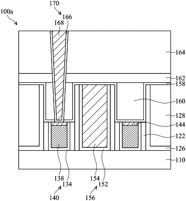
1. A semiconductor device structure, comprising:
a contact etch stop layer (CESL) having a first sidewall CESL portion and a second sidewall CESL portion separated by a spacing;
a gate stack and gate spacers disposed along sidewalls of the gate stack, wherein the gate stack and the gate spacers fill the spacing between a lower portion of the first sidewall CESL portion and a lower portion of the second sidewall CESL portion; and
a dielectric feature disposed over the gate stack and the gate spacers, wherein the dielectric feature fills the spacing between an upper portion of the first sidewall CESL portion and an upper portion of the second sidewall CESL portion, the dielectric feature includes a dielectric layer disposed over a dielectric liner, and the dielectric liner is between the dielectric layer and the gate spacers, between the dielectric layer and the gate stack, and between the dielectric layer and the CESL, and further wherein the dielectric liner extends over a top surface of the first sidewall CESL portion and a top surface of the second sidewall CESL portion.
|