| CPC H01L 29/4175 (2013.01) [H01L 29/66462 (2013.01); H01L 29/7786 (2013.01); H01L 29/0684 (2013.01); H01L 29/2003 (2013.01); H01L 29/205 (2013.01); H01L 29/401 (2013.01)] | 14 Claims |
|
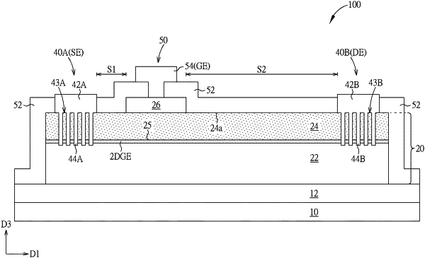
1. A high electron mobility transistor, comprising:
a substrate;
a mesa structure disposed on the substrate, wherein the mesa structure comprises a channel layer, a barrier layer on the channel layer, two opposite first edges extending along a first direction, and two opposite second edges extending along a second direction;
a passivation layer disposed on the mesa structure; and
at least a contact structure disposed in the passivation layer and the mesa structure, wherein the contact structure comprises a body portion and a plurality of protruding portions, the body portion penetrates through the passivation layer and overlaps and directly contacts the two opposite first edges of the mesa structure without overlapping the two opposite second edges of the mesa structure, the plurality of protruding portions penetrate through the barrier layer and a portion of the channel layer.
|