| CPC H01L 29/2003 (2013.01) [H01L 29/66431 (2013.01); H01L 29/7786 (2013.01); H01L 29/7787 (2013.01)] | 10 Claims |
|
1. A manufacturing method of a semiconductor device, comprising:
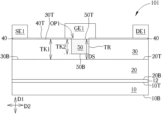
forming a III-V compound barrier layer on a III-V compound semiconductor layer;
forming a gate trench in the III-V compound barrier layer;
forming a p-type doped III-V compound layer in the gate trench, wherein a top surface of the p-type doped III-V compound layer and a top surface of the III-V compound barrier layer are substantially coplanar;
forming an insulation layer on the III-V compound barrier layer before the step of forming the gate trench, wherein the III-V compound semiconductor layer, the III-V compound barrier layer, and the insulation layer are formed on a first region and a second region of a substrate;
forming an opening penetrating through the insulation layer in a vertical direction, wherein the opening is located corresponding to the gate trench in the vertical direction;
forming a first gate electrode on the p-type doped III-V compound layer and the insulation layer, wherein the opening, the gate trench, the p-type doped III-V compound layer, and the first gate electrode are formed on the first region of the substrate; and
forming a second gate electrode on the III-V compound barrier layer located on the second region of the substrate, wherein the first gate electrode and the second gate electrode are formed concurrently by the same process.
|