US 12,266,694 B2
Silicon carbide device with a stripe-shaped trench gate structure
Caspar Leendertz, Munich (DE); Thomas Basler, Chemnitz (DE); Paul Ellinghaus, Unterhaching (DE); Rudolf Elpelt, Erlangen (DE); Michael Hell, Erlangen (DE); Jens Peter Konrath, Villach (AT); Shiqin Niu, Freising (DE); Dethard Peters, Höchstadt (DE); Konrad Schraml, Feldkirchen (DE); and Bernd Leonhard Zippelius, Erlangen (DE)
Assigned to Infineon Technologies AG, Neubiberg (DE)
Filed by Infineon Technologies AG, Neubiberg (DE)
Filed on Dec. 28, 2023, as Appl. No. 18/398,823.
Application 18/398,823 is a continuation of application No. 18/073,860, filed on Dec. 2, 2022, granted, now 11,888,032.
Application 18/073,860 is a continuation of application No. 16/986,338, filed on Aug. 6, 2020, granted, now 11,552,173, issued on Jan. 10, 2023.
Claims priority of application No. 102019121859.4 (DE), filed on Aug. 14, 2019.
Prior Publication US 2024/0136406 A1, Apr. 25, 2024
This patent is subject to a terminal disclaimer.
Int. Cl. H01L 29/16 (2006.01); H01L 29/10 (2006.01); H01L 29/423 (2006.01); H01L 29/78 (2006.01)
CPC H01L 29/1608 (2013.01) [H01L 29/1095 (2013.01); H01L 29/4236 (2013.01); H01L 29/7813 (2013.01)] 27 Claims
OG exemplary drawing
 
1. A silicon carbide device, comprising:
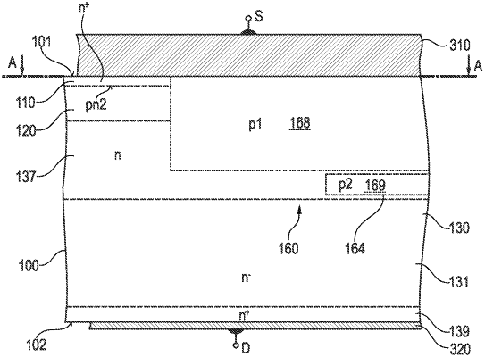
a transistor cell comprising a stripe-shaped trench gate structure extending from a first surface into a silicon carbide body, the gate structure having a gate length along a lateral first direction, a bottom surface and a first gate sidewall of the gate structure being connected via a first bottom edge of the gate structure;
at least one source region of a first conductivity type in contact with the first gate sidewall; and
a shielding region of a second conductivity type in contact with the first bottom edge of the gate structure across at least 20% of the gate length,
wherein no source regions of the first conductivity type are in contact with a second gate sidewall of the gate structure.