| CPC H01L 29/0847 (2013.01) [H01L 21/0262 (2013.01); H01L 29/045 (2013.01); H01L 29/66795 (2013.01); H01L 29/785 (2013.01); H01L 21/0245 (2013.01); H01L 21/02532 (2013.01); H01L 21/02609 (2013.01)] | 20 Claims |
|
1. A method, comprising:
forming a fin protruding from a substrate;
forming an isolation region surrounding the fin;
forming a gate structure extending over the fin and the isolation region;
etching the fin adjacent the gate structure to form a recess;
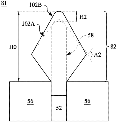
forming a source/drain region in the recess, comprising:
performing a first epitaxial process to grow a first semiconductor material in the recess, wherein the first epitaxial process preferentially forms facet planes of a first crystalline orientation; and
performing a second epitaxial process to grow a second semiconductor material on the first semiconductor material, the second epitaxial process preferentially forms facet planes of a second crystalline orientation that is a different crystalline orientation than the first crystalline orientation, wherein a top surface of the second semiconductor material is above a top surface of the fin, wherein the second semiconductor material has a similar composition as the first semiconductor material; and
forming a source/drain contact on the source/drain region.
|