| CPC H01L 28/60 (2013.01) [H01L 23/5226 (2013.01); H01L 27/0629 (2013.01)] | 20 Claims |
|
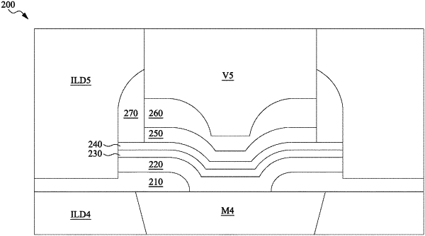
1. A method comprising:
forming a portion of a metallization layer on a substrate;
forming a via layer on the substrate;
forming a first electrode between the metallization layer and the via layer, wherein the first electrode is electrically connected to the metallization layer;
forming a second electrode between the metallization layer and the via layer, wherein the second electrode is electrically connected to the via layer; and
forming a dielectric layer between the first electrode and the second electrode, wherein the first electrode, the dielectric layer, and the second electrode form a metal-insulator-metal (MIM) capacitor;
wherein the first electrode is not electrically connected to any other conductors other than through the metallization layer, and wherein a peripheral boundary of the first electrode encompasses a peripheral boundary of the portion of the metallization layer; and
wherein the second electrode is not electrically connected to any conductors other than through the via layer.
|