| CPC H01L 28/60 (2013.01) [H01G 4/008 (2013.01); H01G 4/012 (2013.01); H01G 4/06 (2013.01); H01G 4/1272 (2013.01); H01G 4/33 (2013.01); H01L 28/90 (2013.01); H10B 12/03 (2023.02); H10B 12/30 (2023.02); H01G 4/1218 (2013.01); H01G 4/1236 (2013.01); H10B 12/033 (2023.02)] | 14 Claims |
|
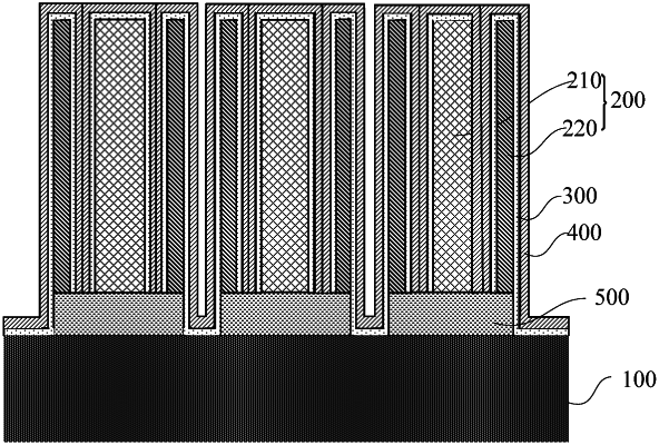
1. A method of manufacturing a capacitor structure, comprising:
providing a substrate;
forming a first conductive structure with a shape of column on the substrate;
forming a second conductive structure on the substrate, wherein the second conductive structure surrounds the first conductive structure and is spaced with the first conductive structure, a cross-section of the second conductive structure is annular, and the first conductive structure and the second conductive structure together form a bottom electrode;
forming a capacitor contact pad, wherein the capacitor contact pad is located between the substrate and the bottom electrode, the bottom electrode is electrically connected with the capacitor contact pad, both of the first conductive structure and the second conductive structure are landing on a top surface of a same capacitor contact pad, and a width of the capacitor contact pad is equal to a width of the second conductive structure;
forming a capacitor dielectric layer, wherein the capacitor dielectric layer covers a surface of the substrate and a surface of the bottom electrode; and
forming a top electrode covering a surface of the capacitor dielectric layer.
|