| CPC H01L 27/156 (2013.01) | 19 Claims |
|
1. A display substrate, comprising:
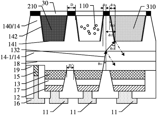
a plurality of light emitting diode chips, wherein each of the plurality of light emitting diode chips comprises a plurality of light emitting units which respectively emit light of different colors, each of the plurality of light emitting units comprises a first electrode, a light emitting layer, a base and a second electrode, wherein the base is located at a side of the light emitting layer away from the second electrode,
wherein, in each of the plurality of light emitting diode chips, the plurality of light emitting units share the base and the first electrode, the light emitting layers of the plurality of light emitting units emit light of a same color, the light of a same color is a first color light, and at least one light emitting unit further comprises a first color conversion layer located at a side of the base away from the light emitting layer, so as to convert the first color light emitted by the light emitting layer into a second color light;
each of the plurality of light emitting units further comprises a first contact pad and a second contact pad which are arranged in a same layer, the first contact pad is connected with the first electrode, and the second contact pad is connected with the second electrode;
each of the plurality of light emitting diode chips comprises a first color light emitting unit, a second color light emitting unit and a third color light emitting unit, the first color light emitting unit is configured to emit the first color light; the second color light emitting unit further comprises the first color conversion layer located at a side of the base away from the light emitting layer and the second color light emitting unit emits the second color light, and the third color light emitting unit further comprises a second color conversion layer at a side of the base away from the light emitting layer, so as to convert the first color light emitted by the light emitting layer into third color light.
|