| CPC H01L 27/156 (2013.01) [H01L 27/124 (2013.01); H01L 33/36 (2013.01); H01L 33/44 (2013.01); H01L 33/62 (2013.01); G09G 3/32 (2013.01); G09G 2300/0426 (2013.01); G09G 2310/0267 (2013.01); G09G 2310/027 (2013.01)] | 20 Claims |
|
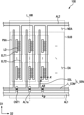
1. A display device, comprising:
a substrate comprising a display area having a plurality of pixel areas and a non-display area located around the display area;
at least one transistor in the plurality of pixel areas on the substrate;
a reference voltage wiring extending from the non-display area to the display area;
first and second pixel electrodes in the plurality of pixel areas on the at least one transistor;
a plurality of light emitting elements on the first pixel electrode and the second pixel electrode;
first and second contact electrodes on the plurality of light emitting elements;
a first wiring on the reference voltage wiring in the non-display area,
wherein the first wiring is directly coupled to the reference voltage wiring in the non-display area, and
wherein the reference voltage wiring is not directly electrically connected to any of the plurality of light emitting elements.
|