| CPC H01L 27/14634 (2013.01) [G02B 6/4253 (2013.01); G02B 6/4274 (2013.01); G02B 6/43 (2013.01); H01L 21/4857 (2013.01); H01L 21/56 (2013.01); H01L 23/3107 (2013.01); H01L 23/367 (2013.01); H01L 23/49822 (2013.01); H01L 23/58 (2013.01); H01L 27/14618 (2013.01); H01L 27/14625 (2013.01); H01L 27/14636 (2013.01); H01L 27/1469 (2013.01)] | 20 Claims |
|
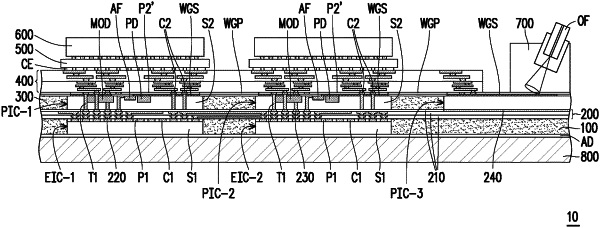
7. A semiconductor package, comprising:
first and second electric integrated circuit dies;
a first insulating encapsulant laterally encapsulating the first and second electric integrated circuit dies;
a first photoelectric integrated circuit die over and electrically connected to the first electric integrated circuit die, the first photoelectric integrated circuit die comprising a first semiconductor waveguide;
a second photoelectric integrated circuit die over and electrically connected to the second electric integrated circuit die, the second photoelectric integrated circuit die comprising a second semiconductor waveguide;
a second insulating encapsulant laterally encapsulating the first and second photoelectric integrated circuit dies; and
a waveguide over the second insulating encapsulant, wherein the waveguide extends from the first semiconductor waveguide of the first photoelectric integrated circuit die to the second semiconductor waveguide of the second photoelectric integrated circuit die.
|