| CPC H01L 27/14621 (2013.01) [H01L 27/14627 (2013.01); H01L 27/1463 (2013.01)] | 20 Claims |
|
1. An image sensor, comprising:
a substrate having a first surface and a second surface opposite to the first surface;
a separation structure penetrating the substrate;
photoelectric conversion device regions spaced apart from each other by the separation structure;
color filters disposed on the second surface of the substrate; and
microlenses disposed on the color filters,
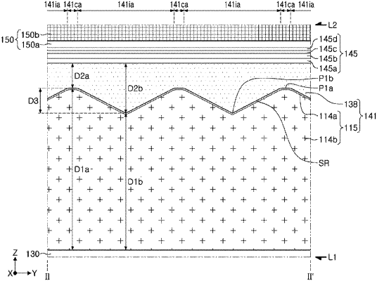
wherein the separation structure includes a lower separation pattern and an upper separation pattern disposed on the lower separation pattern,
wherein the separation structure includes first line portions that are parallel to each other and extend in a horizontal direction, and second line portions perpendicularly intersecting the first line portions, the second line portions being parallel to each other,
wherein in one of the first line portions of the separation structure, an upper surface of the lower separation pattern and/or a lower surface of the upper separation pattern has a wavy or sawtooth shape, and
wherein, in intersecting regions in which the first line portions and the second line portions intersect each other, a vertical length of one of the lower separation pattern and the upper separation pattern is about 2 to about 10 times greater than a vertical length of the other.
|