| CPC H01L 27/1225 (2013.01) [H01L 27/124 (2013.01); H01L 27/1251 (2013.01); H01L 29/24 (2013.01); H01L 29/78672 (2013.01); H01L 29/7869 (2013.01); H01L 29/7881 (2013.01)] | 20 Claims |
|
1. An apparatus comprising:
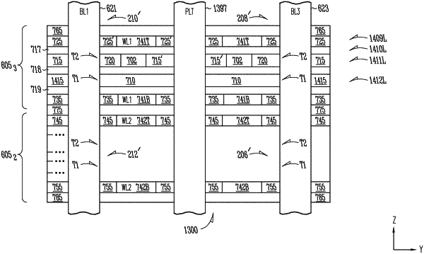
a pillar extending in a first direction;
a first conductive region located in a first level of the apparatus, the first conductive region being separated from the pillar by a first dielectric material located in the first level, first dielectric material being adjacent the first conductive region in a second direction;
a second conductive region located in a second level of the apparatus, the second conductive region being separated from the pillar by a second dielectric material located in the second level;
a memory cell located between the first and second conductive regions and separated from the first and second conductive regions, the memory cell including a first material located in a third level of the apparatus between the first and second levels and coupled to the pillar, and a second material located in a fourth level of the apparatus between the first and second levels and coupled to the pillar, the first and second materials having different conductivity types; and
a conductive connection coupled to the first material.
|