| CPC H01L 27/0886 (2013.01) [H01L 21/02068 (2013.01); H01L 21/02532 (2013.01); H01L 21/3065 (2013.01); H01L 21/823431 (2013.01); H01L 21/823437 (2013.01); H01L 21/823481 (2013.01); H01L 29/0642 (2013.01); H01L 29/161 (2013.01); H01L 29/66545 (2013.01); H01L 29/66795 (2013.01); H01L 29/785 (2013.01)] | 20 Claims |
|
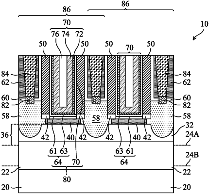
1. An integrated circuit device comprising:
dielectric isolation regions;
a semiconductor fin protruding higher than portions of the dielectric isolation regions on opposite sides of the semiconductor fin;
a silicon cap layer on, and directly contacting both of a top surface and sidewalls of, the semiconductor fin;
a gate stack on the silicon cap layer;
a gate spacer on a sidewall of the gate stack, wherein the gate spacer comprises an inner sidewall contacting the gate stack, and an outer sidewall opposite to the inner sidewall, wherein an edge of the silicon cap layer is recessed in a direction more toward the a center of the gate stack than the outer sidewall of the gate spacer, and wherein the edge of the silicon cap layer and the gate spacer are on a same side of the gate stack, and wherein in a top view of the gate spacer and the gate stack, the direction points from the outer sidewall to the inner sidewall, and the direction is perpendicular to a longitudinal direction of the gate spacer in the top view; and
a source/drain region contacting the semiconductor fin and the edge of the silicon cap layer.
|