| CPC H01L 27/0886 (2013.01) [H01L 21/28114 (2013.01); H01L 21/823431 (2013.01); H01L 21/823437 (2013.01); H01L 21/823468 (2013.01); H01L 21/823481 (2013.01); H01L 29/41791 (2013.01); H01L 29/42376 (2013.01); H01L 29/66545 (2013.01); H01L 29/6656 (2013.01); H01L 29/66795 (2013.01); H01L 29/7851 (2013.01); H01L 29/4991 (2013.01)] | 20 Claims |
|
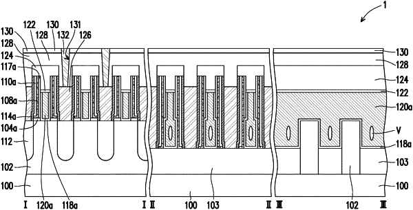
1. A FinFET device, comprising:
a substrate having fins;
a metal gate strip disposed across the fins and having a reversed T-shaped portion in a cross section cut between two adjacent fins along an extension direction of the fins, wherein a portion of the reversed T-shaped portion is embedded between the two adjacent fins;
multiple gate spacers disposed on a first sidewall of the metal gate strip;
a T-shaped dielectric helmet disposed over the metal gate strip;
an interfacial layer disposed below the multiple gate spacers, wherein laterally opposite sidewalls of the interfacial layer are flush with sidewalls of the multiple gate spacers; and
an etch stop layer disposed on the first sidewall of the metal gate strip covering the multiple gate spacers, wherein outer sidewalls of the T-shaped dielectric helmet are flush with sidewalls of the etch stop layer.
|