| CPC H01L 27/088 (2013.01) [H01L 21/823418 (2013.01); H01L 21/823468 (2013.01); H01L 21/823475 (2013.01)] | 20 Claims |
|
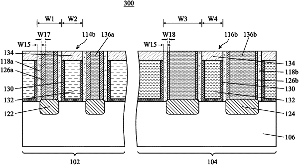
1. A semiconductor structure comprising:
a first semiconductor device formed over a substrate comprising:
a first source/drain feature over the substrate;
a first gate structure over the substrate;
a first conductive feature over the first source/drain feature; and
a first insulation layer between the first gate structure and the first conductive feature, wherein the first insulation layer comprises a first contact etching stop layer (CESL) in contact with the first source/drain feature; and
a second semiconductor device formed over the substrate comprising:
a second source/drain feature over the substrate;
a second gate structure over the substrate;
a second conductive feature over the second source/drain feature; and
a second insulation layer between the second gate structure and the second conductive feature, the second insulation layer comprises a second CESL in contact with the second source/drain feature,
wherein a thickness of the first CESL is less than a thickness of the second CESL.
|