| CPC H01L 27/088 (2013.01) [H01L 21/76232 (2013.01); H01L 21/823418 (2013.01); H01L 21/823481 (2013.01)] | 19 Claims |
|
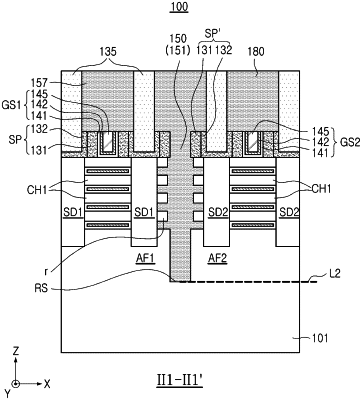
1. A semiconductor device comprising:
a substrate including a first active fin and a second active fin each extending in a first direction and arranged on a first line, the substrate having a recess between the first active fin and the second active fin;
a device isolation film on the substrate and surrounding a first portion of the first active fin and a second portion of the second active fin;
a first gate structure and a second gate structure on the first active fin and the second active fin, respectively, and extending in a second direction, intersecting the first direction; and
a field separation layer having a first portion located between the first active fin and the second active fin and in the recess, and a second portion extending from both sides of the first portion in the second direction to an upper surface of the device isolation film,
wherein the recess has a bottom surface lower in a third direction intersecting the first direction and the second direction than the upper surface of the device isolation film, and
a first region of the upper surface of the device isolation film, in which the second portion of the field separation layer is located, has a flat surface and is lower in the third direction than a second region of the upper surface of the device isolation film in which the first and second gate structures are positioned.
|