| CPC H01L 25/167 (2013.01) [H01L 23/5384 (2013.01); H01L 33/52 (2013.01); H01L 33/58 (2013.01); G02B 6/4206 (2013.01)] | 20 Claims |
|
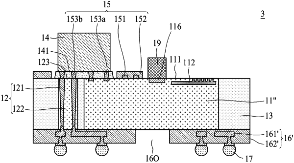
1. A semiconductor device package, comprising:
a first semiconductor device having a first surface and a second surface opposite to the first surface, wherein the first semiconductor device is substantially transmissive to a first light;
a light emitting device disposed over the second surface of the first semiconductor device;
a multilayer structure disposed under the first surface of the first semiconductor device and having an opening vertically overlapping the first semiconductor device and the light emitting device,
wherein the opening is configured to allow a second light to pass substantially vertically through the first semiconductor device and towards the light emitting device.
|