| CPC H01L 25/0657 (2013.01) [H01L 24/02 (2013.01); H01L 24/03 (2013.01); H01L 24/05 (2013.01); H01L 24/08 (2013.01); H01L 25/105 (2013.01); H01L 25/50 (2013.01); H01L 24/06 (2013.01); H01L 24/73 (2013.01); H01L 2224/02141 (2013.01); H01L 2224/0311 (2013.01); H01L 2224/0312 (2013.01); H01L 2224/05559 (2013.01); H01L 2224/0557 (2013.01); H01L 2224/05573 (2013.01); H01L 2224/05647 (2013.01); H01L 2224/06135 (2013.01); H01L 2224/08225 (2013.01); H01L 2224/73204 (2013.01); H01L 2225/06513 (2013.01); H01L 2225/06544 (2013.01); H01L 2225/06548 (2013.01); H01L 2225/06586 (2013.01); H01L 2225/1035 (2013.01); H01L 2225/1058 (2013.01)] | 20 Claims |

|
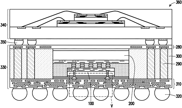
1. A method of fabricating a semiconductor package, comprising:
bonding a first semiconductor substrate having a through substrate via to a second semiconductor substrate;
encapsulating the first semiconductor substrate using a first insulating encapsulation on the second semiconductor substrate;
removing a portion of the first semiconductor substrate until revealing a portion of the through substrate via and forming a concave structure laterally spaced from the first insulating encapsulation by a portion of the first semiconductor substrate while the portion of the first semiconductor substrate and the first insulating encapsulation are covered by a protection layer;
forming a dielectric layer structure on the first semiconductor substrate and the first insulating encapsulation;
forming a conductor structure extending through the dielectric layer structure and electrically connected to the through substrate via; and
forming a second insulating encapsulation in contact with a side edge of the second semiconductor substrate, a side edge of the first insulting encapsulation, and a side edge of the dielectric layer structure.
|