| CPC H01L 25/0655 (2013.01) [H01L 23/3185 (2013.01); H01L 23/562 (2013.01); H01L 24/16 (2013.01); H01L 25/50 (2013.01); H01L 2224/16157 (2013.01)] | 20 Claims |
|
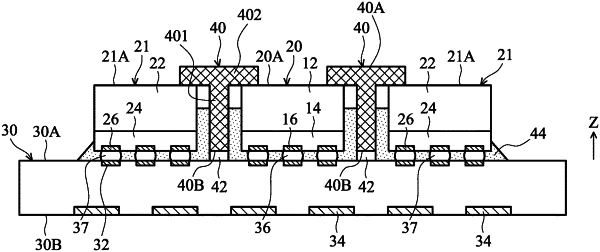
1. A semiconductor device package, comprising:
a substrate;
a first package component and a second package component disposed over and bonded to the substrate, wherein the first and second package components are different types of electronic components that provide different functions;
at least one dummy die disposed over and attached to the substrate, wherein the dummy die is between the first and second package components and is electrically isolated from the substrate, and
wherein the dummy die has a first portion between adjacent sidewalls of the first and second package components and attached to the package substrate, and a second portion extending continuously from the first portion to top surfaces of the first and second package components; and
an underfill element disposed between the substrate, the first package component, the second package component and the at least one dummy die, wherein the underfill element has a maximum height lower than a bottom surface of the second portion of the dummy die.
|