| CPC H01L 25/0652 (2013.01) [H01L 23/3135 (2013.01); H01L 23/49816 (2013.01); H01L 24/27 (2013.01); H01L 24/32 (2013.01); H01L 24/33 (2013.01); H01L 24/48 (2013.01); H01L 2224/32145 (2013.01); H01L 2224/33517 (2013.01); H01L 2224/33519 (2013.01); H01L 2224/48225 (2013.01)] | 20 Claims |
|
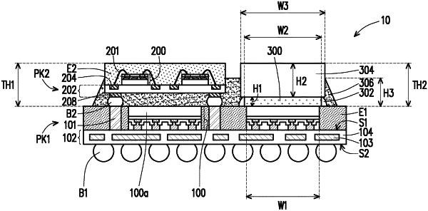
1. A semiconductor structure, comprising:
a first semiconductor package comprising a plurality of dies laterally disposed side by side;
a second semiconductor package disposed over and corresponding to a first one of the plurality of dies;
a heat spreader disposed over and corresponding to a second one of the plurality of dies; and
a dielectric layer disposed over the first semiconductor package and around the second semiconductor package and the heat spreader.
|