| CPC H01L 24/13 (2013.01) [H01L 24/03 (2013.01); H01L 24/05 (2013.01); H01L 24/11 (2013.01); H01L 24/16 (2013.01); H01L 24/29 (2013.01); H01L 24/32 (2013.01); H01L 24/73 (2013.01); H01L 24/81 (2013.01); H01L 24/83 (2013.01); H01L 24/92 (2013.01); H01R 4/58 (2013.01); H01R 43/00 (2013.01); H01L 2224/0345 (2013.01); H01L 2224/05573 (2013.01); H01L 2224/1146 (2013.01); H01L 2224/13016 (2013.01); H01L 2224/13082 (2013.01); H01L 2224/13109 (2013.01); H01L 2224/13111 (2013.01); H01L 2224/13147 (2013.01); H01L 2224/16057 (2013.01); H01L 2224/2919 (2013.01); H01L 2224/321 (2013.01); H01L 2224/73204 (2013.01); H01L 2224/81201 (2013.01); H01L 2224/81898 (2013.01); H01L 2224/81948 (2013.01); H01L 2224/83102 (2013.01); H01L 2224/83855 (2013.01); H01L 2224/9205 (2013.01); H01L 2924/0665 (2013.01); H01L 2924/20104 (2013.01); H01L 2924/20105 (2013.01); H01L 2924/20106 (2013.01); H01L 2924/20107 (2013.01); H01L 2924/20108 (2013.01)] | 20 Claims |
|
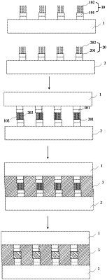
1. A substrate bonding method, wherein the substrate bonding method comprises steps of:
providing a first substrate and a second substrate;
forming a first metal micro-bump array on the first substrate, wherein the first metal micro-bump array comprises at least one first metal pillar formed on the first substrate and a plurality of first metal nanowires formed on the first metal pillar and spaced apart from each other;
forming a second metal micro-bump array on the second substrate, wherein the second metal micro-bump array comprises at least one second metal pillar formed on the second substrate and a plurality of second metal nanowires formed on the second metal pillar and spaced apart from each other;
pressing the first substrate onto the second substrate, such that the first metal micro-bump array and the second metal micro-bump array are positioned in a manner of being staggered with each other, hereby forming a physically interwoven interlocking structure between the first metal nanowires and the second metal nanowires;
applying a filling material between the first substrate and the second substrate;
curing the filling material to form a bonding cavity; and
performing heating confinement reflux on the first metal micro-bump array and the second metal micro-bump array in the bonding cavity, after the filling material is cured, so as to realize bonding of the first substrate and the second substrate.
|