| CPC H01L 23/66 (2013.01) [H01L 21/4853 (2013.01); H01L 21/4857 (2013.01); H01L 21/561 (2013.01); H01L 21/565 (2013.01); H01L 21/568 (2013.01); H01L 21/6835 (2013.01); H01L 21/6836 (2013.01); H01L 21/78 (2013.01); H01L 23/3114 (2013.01); H01L 23/3128 (2013.01); H01L 23/5383 (2013.01); H01L 23/5384 (2013.01); H01L 23/5386 (2013.01); H01L 23/5389 (2013.01); H01L 23/552 (2013.01); H01L 24/19 (2013.01); H01L 24/20 (2013.01); H01L 24/96 (2013.01); H01L 25/105 (2013.01); H01L 25/50 (2013.01); H01P 3/003 (2013.01); H01Q 1/2283 (2013.01); H01Q 1/38 (2013.01); H01Q 9/0457 (2013.01); H01L 21/486 (2013.01); H01L 2221/68331 (2013.01); H01L 2221/68359 (2013.01); H01L 2221/68372 (2013.01); H01L 2223/6616 (2013.01); H01L 2223/6627 (2013.01); H01L 2223/6677 (2013.01); H01L 2224/214 (2013.01); H01L 2224/95001 (2013.01); H01L 2224/97 (2013.01); H01L 2225/1035 (2013.01); H01L 2225/1058 (2013.01); H01L 2924/3025 (2013.01); H01Q 21/065 (2013.01)] | 20 Claims |
|
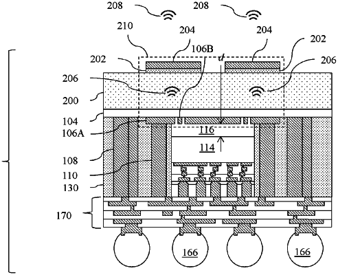
1. A package comprising:
an integrated circuit die encapsulated in an encapsulant;
a patch antenna device over the integrated circuit die, wherein the patch antenna device overlaps the integrated circuit die in a top-down view, and wherein the patch antenna device comprises a ground element and a signal line disposed in a same layer; and
a dielectric feature disposed between the integrated circuit die and the patch antenna device, wherein the dielectric feature is in direct contact with the integrated circuit die, wherein a thickness of the dielectric feature is selected based on an operating bandwidth of the patch antenna device, wherein the dielectric feature is encapsulated in the encapsulant.
|