| CPC H01L 23/66 (2013.01) [H01L 23/49816 (2013.01); H01L 23/552 (2013.01); H01Q 1/2283 (2013.01); H01L 21/565 (2013.01); H01L 25/165 (2013.01); H01L 2223/6616 (2013.01); H01L 2223/6677 (2013.01); H01L 2223/6688 (2013.01); H01Q 1/38 (2013.01)] | 18 Claims |
|
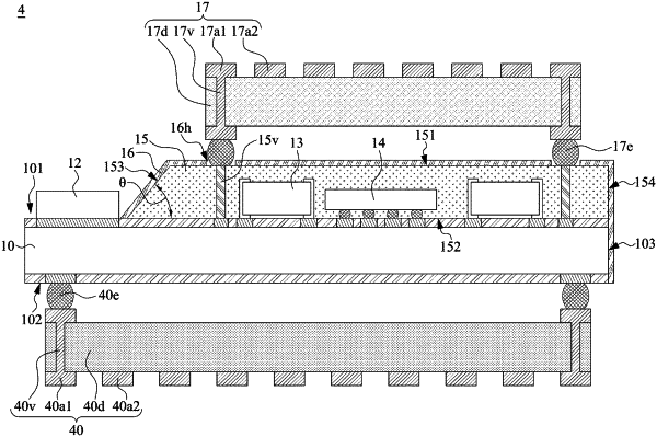
1. A semiconductor device, comprising:
a carrier having a first side and a second side opposite to the first side;
a first antenna array disposed over the first side and configured to operate at a first frequency; and
a second antenna array disposed under the second side and configured to operate at a second frequency different from the first frequency;
a conductive element disposed over the first side of the carrier, wherein the first antenna array is electrically connected to the conductive element by a solder material.
|